Tag Archives: Radio Waves

How America Launched The Digital Age

Modern conveniences many take for granted — cell phones, laptops, GPS devices, even coffee makers — run on computer chips introduced by U.S. firms that established America’s leading role in technology. Trace the digital revolution, from its beginnings to the present day, with each groundbreaking advance.

How did these gains happen? Today’s technology emerged from U.S. support for research and development combined with America’s robust private sector, its scientific community, and its innovative spirit.

Bell Labs, a legendary research hub in New Jersey, began as a branch of the Western Electric Company, a subsidiary of the American Telephone and Telegraph Company (AT&T).

Founded in 1925 to meet a growing need for mass communications, Bell Labs hired top engineers, physicists, chemists, and mathematicians to design and patent equipment (including a high-vacuum tube that transmitted telephone signals across North America).

Bell Labs encouraged interdisciplinary collaboration that produced groundbreaking discoveries. The labs were driven by scientific curiosity, flexible deadlines, and — thanks to AT&T’s budget — stable funding. Lab directors adopted a hands-off management style, and innovation flourished.

Karl Jansky sits beside his large rotating radio antenna used to detect cosmic radio waves, 1930s. (© Bettmann/Getty Images)

DID YOU KNOW?

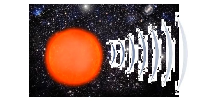
In 1932, Bell Labs physicist Karl Jansky discovered radio waves coming from outer space. He’s known as the father of radio astronomy.

Karl Jansky’s pioneering radio antenna at Bell Labs revealed signals from the Milky Way — launching radio astronomy. (© Bettmann/Getty Images)

In the post-World War II period, Bell Labs’ Mervin Kelly assembled an all-star team of scientists to develop a replacement for the vacuum tube, which was bulky, fragile, and prone to burning out.

In 1947, John Bardeen and Walter Brattain — supervised by fellow physicist William Shockley — invented the point-contact transistor, a semiconductor device that amplifies sound and switches electrical currents on and off.

In 1948, Shockley designed the junction transistor, a more robust and reliable transistor. Its small size, low power consumption, and durability paved the way for computers, portable radios, cell phones, and other devices.

Eight years later, Bardeen, Brattain, and Shockley would be awarded the Nobel Prize in physics for this breakthrough.

William Shockley receives Nobel Prize medal from King Gustav VI Adolph in Stockholm, 1956. (© AFP/Getty Images)

DID YOU KNOW?

Bell Labs researchers have been awarded 10 Nobel Prizes in physics and chemistry, spanning from 1937 to 2023. While Bell Labs was at its most productive from the 1940s to the 1970s, important research continues today at its New Jersey headquarters.

William Shockley accepts the 1956 Nobel Prize for his role in developing the transistor. (© AFP via Getty Images)

Bell Labs continued to improve transistor technology during the 1950s, developing the silicon transistor and the metal-oxide-semiconductor field-effect transistor (MOSFET).

The MOSFET proved crucial for building high-density integrated circuits (ICs), or microchips, in the 1960s. Microchips — consisting of billions of tiny transistors crafted from semiconductor materials, commonly silicon — work together to power electronics.

Recognizing the potential for widespread impact and profits, Bell Labs created licensing agreements to share transistor technology with other companies.

In 1955, William Shockley left Bell Labs to establish Shockley Semiconductor Laboratory in Mountain View, California. Within a couple of years, some of his employees — engineers and scientists — formed their own company, Fairchild Semiconductor.

Fairchild is credited with the birth of Silicon Valley. The company became a major player in the growing semiconductor industry, and many Silicon Valley firms — including Intel (founded in 1968) and Apple (in 1976) — have ties to Fairchild alumni to this day.

Close-up of a small integrated-circuit chip with gold connectors, 1981 (© David Madison/Getty Images)

As demand for semiconductors grew, so did the need for manufacturing capabilities.

Throughout the 1980s and 1990s, Japan, South Korea, and Taiwan became players in the industry, with Japanese companies like Toshiba and NEC influencing the data-storage market and South Korea’s Samsung and SK Hynix focusing on memory-chip production.

Meanwhile, the Taiwan Semiconductor Manufacturing Company (TSMC) upended a traditional business model of integrating chip design and manufacturing. It introduced the fabless-foundry model, encouraging firms to specialize in either design (fabless) or fabrication/manufacturing (foundry).

This increased efficiency. What’s more, it allowed many small firms — those lacking resources to open manufacturing plants — to design chips.

Engineers push trolleys carrying wafer pods inside semiconductor fabrication plant in Taiwan, 2006. (© Sam Yeh/AFP/Getty Images)

DID YOU KNOW?

The fabless-foundry business model democratized chip production, allowing startups to enter the market without the need for expensive manufacturing facilities.

Engineers at Taiwan’s UMC factory move wafers through one of the world’s leading chip foundries. (© Sam Yeh/AFP/Getty Images)

Experts predict that quantum computing — with its ability to accelerate AI by overcoming limitations on data size, complexity, and processing speeds — will shape the future.

Quantum AI will develop algorithms that could advance pharmaceutical discoveries, predict financial outcomes, improve manufacturing, and bolster cybersecurity. Quantum/AI partnerships already comprise an active and developing market, with U.S. tech giants like IBM and Nvidia investing in both domains.

Bell Labs is born.

Karl Jansky sits beside his large rotating radio antenna used to detect cosmic radio waves, 1930s. (© Bettmann/Getty Images)

Karl Jansky’s pioneering radio antenna at Bell Labs revealed signals from the Milky Way — launching radio astronomy. (© Bettmann/Getty Images)

William Shockley receives Nobel Prize medal from King Gustav VI Adolph in Stockholm, 1956. (© AFP/Getty Images)

William Shockley accepts the 1956 Nobel Prize for his role in developing the transistor. (© AFP via Getty Images)

Close-up of a small integrated-circuit chip with gold connectors, 1981 (© David Madison/Getty Images)
Engineers push trolleys carrying wafer pods inside semiconductor fabrication plant in Taiwan, 2006. (© Sam Yeh/AFP/Getty Images)
Close-up of an Intel 300 mm silicon wafer showing colorful microchip patterns, photographed in Tokyo, 2007 (© Yoshikazu Tsuno/AFP/Getty Images)
Micron Technology logo displayed on modern building exterior in San Jose, 2025. (© Justin Sullivan/Getty Images)
Close up of Google’s quantum processor (© Google)

Afterword:
America’s Approach to Innovation

Industry leaders point to many factors that shape U.S. technological innovation. One such factor is the U.S. system of intellectual property protection, which fosters the spirit of risk-taking, says Walter Copan. (That system is enshrined in the U.S. Constitution, thanks to the foresight of America’s Founding Fathers.)

Sanjay Mehrotra cites the U.S. business culture of “openly, freely being able to debate ideas,” adding, “The best ideas win.”

Thomas Caulfield says, “This is where you can work hard, live your dream, become an entrepreneur, start a company.”

And Jon Gertner notes that key people at Bell Labs came from humble beginnings: “To me, that feels uniquely American — the idea that talent could rise from almost anywhere and shape the future of communications.”

Suburban house and garage in Los Altos where Apple was founded, 2011 photo (© Kevork Djansezian/Getty Images)

Seen here is the modest garage where Steve Jobs and Steve Wozniak built the first Apple computer — an icon of American ingenuity. (© Kevork Djansezian/Getty Images)

DID YOU KNOW?

It’s part of Silicon Valley lore that massive tech empires often sprouted from humble roots. As quantum computing and AI herald the next seismic shifts in technology, innovation hubs could emerge in unlikely places. Who knows? The next great U.S. tech companies might now be incubating in a town anywhere in America.


Additional Photo Credits:
(Library of Congress/Gottscho-Schleisner), (Bell Telephone Magazine), (© James Leynse/Corbis/Getty Images), (Computer History Museum/Beckman Foundation), (© Bettmann/Getty Images), (© Roslan Rahman/AFP/Getty Images), (© Brownie Harris/Getty Images), (Courtesy of Walter Copan), (© Caitlin O’Hara/The Washington Post/Getty Images), (© Mandel Ngan/AFP/Getty Images), (© Angela Weiss/AFP/Getty Images), (Courtesy of Walker Steere)

Featured image- Intel chief executive Brian Krzanich meets with President Trump at the White House in 2017 to announce a $7 billion usd/ $9.73 billion cad investment in a new Arizona factory — one of several commitments to U.S. chip manufacturing. (© Chris Kleponis/Getty Images)

Writer: Lauren Monsen
Photo editor: Serkan Gurbuz
Graphic designer: Buck Insley
Video project manager: Afua Riverson
Video producer: William Leitzinger
Production editor: Kathleen Hendrix
Digital storyteller: Pierce McManus

SETI Search For Space Aliens Increases Odds With Your Computer

Zuhra Abdurashidova
Zuhra Abdurashidova

I graduated from the University of California at Berkeley about a decade ago with a degree in Mechanical Engineering. I received two job offers, one from SETI to work on high performance signal processing and the other from industry.

One does not simply walk away from SETI, so I had the pleasure of joining the Berkeley SETI Research Center (BSRC). I received a warm welcome and was promptly sent to West Virginia to help install a new SETI system at the Green Bank Telescope.

There was a steep learning curve, but I was fascinated by BSRC’s work and couldn’t wait to actually understand what was going on.

As it turns out, our group is looking to expand its computing power, providing the ability to look at more star systems with habitable planets, expand the involvement of volunteers and acquire larger volumes of data; in short, broaden the search and increase our chances of intercepting a signal. Now I’m working on setting up new servers, network hardware, and signal-processing systems at Green Bank. We’re hoping to get data flowing and recording soon, and make it available for the interested public.

From the 19th-century idea of drawing a giant Pythagorean triangle in the Siberian tundra to signal extraterrestrials, to our current collection of servers storing and analyzing data, it is not hard to see how much progress has already been made.

Running SETI software on your home computer looks like this.

Funding from the Breakthrough Initiatives is spawning new projects that would not have been otherwise possible. SETI@home is planning to work with Breakthrough Listen to collect and distribute data from the Green Bank and Parkes telescopes. However, in order to sustain the whole SETI@home effort we could still use support from our devoted SETI@home contributors.

Recently, I spent a day at the Bay Area Science Festival talking to kids and their adults. I was fascinated by just how stoked kids are about SETI. Some came with prepared questions and showed incredible curiosity and intelligence. The BSRC team is hoping to inspire kids to pursue science careers and I think searching for life beyond Earth is a great way to get them interested and involved. I hope you continue your support for this fascinating endeavor, and keep your eyes on the stars.  For the Berkeley SETI Research Center team, Zuhra Abdurashidova.

Berkeley SETI Research Center Logo

Supplemental- via nemesis maturity YouTube channel

Wow Signal – Scientists say that if the signal came from extraterrestrials, they are likely to be an extremely advanced civilization, as the signal would have required a 2.2-gigawatt transmitter, vastly more powerful than any on Earth.

The signal bore the expected hallmarks of non-terrestrial and non-Solar System origin.

One summer night in 1977, Jerry Ehman, a volunteer for SETI, or the Search for Extraterrestrial Intelligence, may have become the first man ever to receive an intentional message from an alien world. Ehman was scanning radio waves from deep space, hoping to randomly come across a signal that bore the hallmarks of one that might be sent by intelligent aliens, when he saw his measurements spike.

The signal lasted for 72 seconds, the longest period of time it could possibly be measured by the array that Ehman was using. It was loud and appeared to have been transmitted from a place no human has gone before: in the constellation Sagittarius near a star called Tau Sagittarii, 122 light-years away.

All attempts to locate the signal again have failed, leading to much controversy and mystery about its origins and its meaning.

http://en.wikipedia.org/wiki/Wow!_signal

http://en.wikipedia.org/wiki/Tau_Sagi…

http://www.bigear.org/wowmenu.htm

5G Technology And Induction Of Coronavirus Into Skin Cells

NOTE- the journal paper was retracted by the author a few days after receiving publication. We do not hold that the paper is factual or not, only that the content is interesting and deserves speculative consideration.

In this research, we show that 5G millimeter waves could be absorbed by dermatologic cells acting like antennas, transferred to other cells and play the main role in producing Coronaviruses in biological cells. DNA is built from charged electrons and atoms and has an inductor-like structure. This structure could be divided into linear, toroid and round inductors. Inductors interact with external electromagnetic waves, move and produce some extra waves within the cells. The shapes of these waves are similar to
shapes of hexagonal and pentagonal bases of their DNA source. These waves produce some holes in liquids within the nucleus. To fill these holes, some extra hexagonal and pentagonal bases are produced.

These bases could join to each other and form virus-like structures such as Coronavirus. To produce these viruses within a cell, it is necessary that the wavelength of external waves be shorter than the size of the cell. Thus 5G millimeter waves could be good candidates for applying in constructing virus-like structures such as Coronaviruses (COVID-19) within cells.

Coronavirus disease (COVID-19) is the main problem this year involving the entire world (1- see full PDF below).

This is an infectious disease caused by a newly discovered coronavirus. This virus is a member of related viruses that cause diseases in mammals and birds. In humans, coronaviruses cause respiratory tract infections that can be mild, such as some cases of the common cold (among other possible causes, predominantly rhinoviruses), and others that can be lethal, such as SARS, MERS, and COVID-19.

Among them, COVID-19 is an enveloped virus with a positive-sense single-stranded RNA genome and a nucleocapsid of helical symmetry. The genome size of coronaviruses ranges from approximately 27 to 34 kilobases, the largest among known RNA viruses (2, 3 see full PDF below). To date, many scientists have tried to find a method to cure this disease (4, 5 see full PDF below); however, without success.

COVID-19 may have effects on different types of cells. For example, it has been argued that this virus may have some effects on dermatologic cells (6 see full PDF below). On the other hand, it has been known that some waves in 5G technology have direct effects on the skin cells (7 see full PDF below).

Thus, there are some similarities between effects of COVID-19 and waves in 5G technology.

A new question arises regarding a relationship between 5G technology and COVID-19. The 5G technology is the fifth-generation mobile technology in which its frequency spectrum could be divided into millimeter waves, mid-band, and low-band. To find out how this may cause the creation of COVID-19 in human cells continue here to read the full PDF.

Silo article via – Biolife 0393-974X (2020)
Copyright © by BIOLIFE, s.a.s.
This publication and/or article is for individual use only and may not be further reproduced without written permission from the copyright holder.
Unauthorized reproduction may result in financial and other penalties
DISCLOSURE: ALL AUTHORS REPORT NO CONFLICTS OF
INTEREST RELEVANT TO THIS ARTICLE. 3
JOURNAL OF BIOLOGICAL REGULATORS & HOMEOSTATIC AGENTS Vol. 34, no. 4, xx-xx (2020)

Dr Massimo Fioranelli,
Department of Nuclear,
Sub-nuclear and Radiation Physics,
Guglielmo Marconi University,
Via Plinio 44-00193, Rome, Italy
e-mail: [email protected]
5G Technology and induction of coronavirus in skin cells
M. Fioranelli1, A. Sepehri1, M.G. Roccia1, M. Jafferany2, O. Yu. Olisova3,
K.M. Lomonosov3 and T. Lotti1,3
1Department of Nuclear, Sub-nuclear and Radiation Physics, G. Marconi University, Rome, Italy;
2Central Michigan Saginaw, Michigan , USA; 3Department of Dermatology and Venereology, I.M.
Sechenov First Moscow State Medical University, Moscow, Russia

New Wearable For Pets Is Lifesaver When Animal Is Lost Or Injured

Next to our children, our pets are some of the most important members of our families. We do everything we can to make sure both our kids and pets are safe, but eventually kids can shoulder some of the burden themselves. But when “Spot” runs off, we can’t expect him to tell the nice neighbor that finds him that he has a medical condition, or who his veterinarian or owner is.

Though your pet will never learn to talk, there is a way to provide whoever finds your lost -or injured- pet with the information they need to offer aid. A new ‘wareable’ technology, MyEndlessID Pet, gives veterinarians and good samaritans all of the information they need to render aid in an emergency.

Inventor- Gustavo Rubacha

“Even the best trained pets might head off on an adventure sometime,” said Gustavo Rubacha, one of MyEndlessID Pet’s inventors. Worse still, Rubacha notes, is that from time to time those ‘adventures’ can result in injuries, sometimes serious.  “We believe that it’s important to prepare for these emergencies ahead of time and that’s why we created MyEndlessID Pet.”

MyEndlessID Pet jams the latest Near-Field Communication (NFC) technology into a tag small enough to hang from a pet’s collar. Utilizing the same tech that until now has only seen mass deployment in payment systems like Apple Pay and Google Wallet, the NFC tag will emit radio waves to any capable smart phone held close to it, providing vital information about your pet with just a tap.

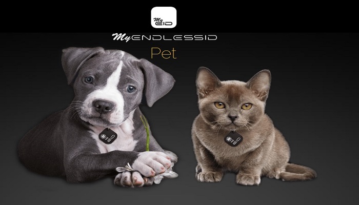
When the device is activated, pet owners receive immediate alerts by text, email and a phone call, along with a geolocation of where their pet is located when the tag is activated. Most importantly though, MyEndlessID Pet provides rescuers and veterinarians instant access to vital medical information that could save an animal’s life in an emergency.

Vital information including medical conditions, medications, vaccinations, allergies, medical history and veterinarian history, insurance information, and more are all instantly available with the simple tap of any modern smartphone.

Unlike an implanted microchip, MyEndlessID Pet does not require special equipment beyond a smartphone to work, and priced at $20USD it is far more affordable than a vet visit to have a device implanted.  And unlike recently introduced ‘smart collars’ – MyEndlessID Pet never requires charging or battery changes.

MyEndlessID Pet is also water resistant, allowing it to withstand whatever mischief your pet might wander into, while continuing to deliver critical information when someone comes to help your pet get out of whatever mess he or she has found himself in. For the Silo, Timothy Williams.